Custom PCB HTCC-AM02 on KiCad

First of all, happy new year to all the geeks here!
I’m a french biologist so please take consideration that electronics stay a hobby to me, maybe my questions to community will help other users and improve IoT.

I really considering making a small batch of custom PCB for plant monitoring -personnal use, non commercial.
During my tests, I success to have running HTCC-AB01/HTCC-AB02 with solars panels, Li-Po batteries and sensors like SHT31 or BME monitoring.
I use Heltec HT-M00 gatewayHT-M00 via TTN and getting my datas periodically with the combo TTN mqtt/NodeRed/Influxdb/Grafana. All of these running on a Raspbery Pi.
I will eventually share my sources for doing that praticaly but Andreas Spiess make a video last year that help me a lot InfluxDB/Grafana from Andreas Spiess
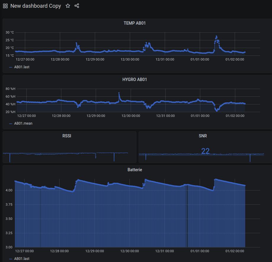
Please keep in mind that I’am not a programmer or IT guy but I love these subjects especially when it works! There is a screen shot of a quick dashboard made in Grafana for the proof of concept.

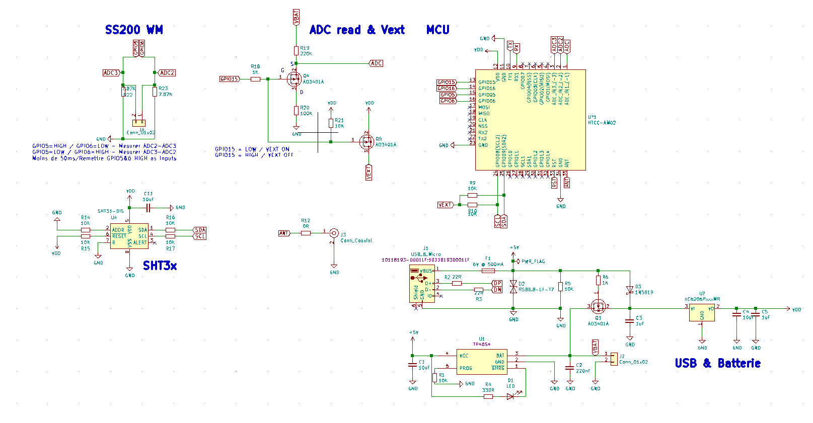
I have a 3D printer and I will make a custom case to integrate solar panel (5.5V/6V), custom PCB with HTCC-AM02, maybe custom antenna. My goal is to integrate this on top of an irrometer 200SS Watermark sensor.
@avalente Help me a lot for the pratical use with the ADC pins of the Cubecell modules please read his publication Low-Cost LoRaWAN Node for Agro-Intelligence IoT

I read a lot about Kicad and on this forum and @jasonXu @jackyruth @Sivaelid and find interestings posts especially Custom PCB reflow

As I aldredy say, this is a hobby and I offer myself a binocular microscope and micro soldering irons.
Do you have recommandations for my future design in Kicad. I make a pre-draft in Kicad just to start to copy circuitery from Reference design Does the documentations ar good to go for PCB design or it contains small errors ?

My questions are in bulk:

-Should I stricly copy the recommended design (Boot circuit, usb interface) or simplify my circuit with an external pogo jig programmer (I have aldrady made one with 3d printer for another project) and get rid of the maximum components like buttons?

-I will mature my design of Kicad and I will order a batch of 5 PCB on Jlcpcb. Some of components from the reference design seems to not appear on the Jlcpb assembly service.
Time for deliveries are not an issue for me, so will I prefer order my PCB assembled or sourcing each parts from differents sellers and solder myself?Again, I’m a newbie for finding alternatives to a proposed components so maybe some of you can share how you solve this type of issues for your PCB design. (I love soldering and I want to make the most of steps of the project). LCSC JLCPCB assembly parts

Do you have advices to start a design from scratch. I think one of my goal is to get a Pcb with the smalest footprint possible and get rid of the maximum components just to have the smallest case poissible on top of my irometer… I will only conserve these parts.
-HTCC AM02
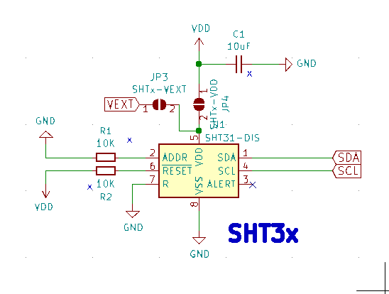
-SHT31 or another temp/hygro sensor
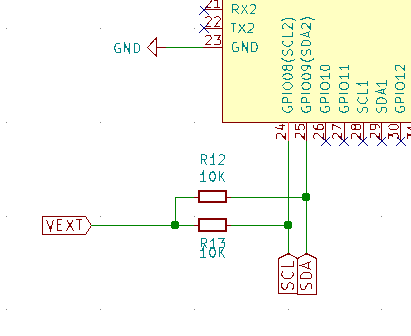
-Using ADC’s from the module to read only one irrometer Watermark value.
-Solar charging and solar panel
-Bootloader Autoboot circuit (if necessary)
-Usb side for programming or external pogo pins connectors.
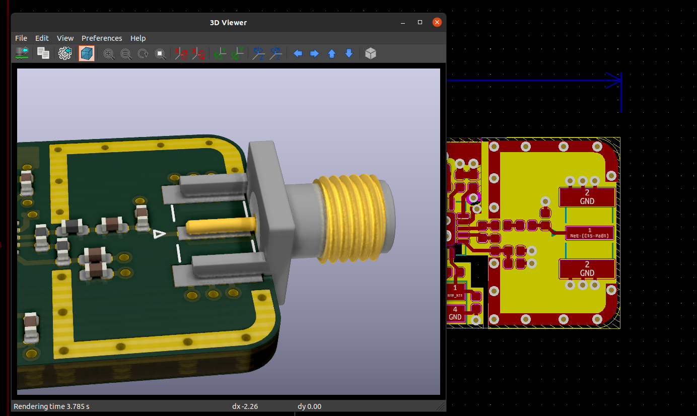
-Integrate RF circuitery correctly and add an SMA connector for external antennas.
-One cell battery (18650 or small LiPo that I have on my dev boards running well).

I dig some interestings videos on PCB design in Kicad and I think to adopt a similar pcb form factor
Kicad sources STRF Video tutorial I know some of you are proffessionals but this type of video helps a lot to understand PCB designs software and manufacturers requirements for order a small batch of PCB.

Making the 3D print case on top of the irrometer and waterproofing electronics will be final steps but I have experience from past projects.

What kind of difficulties/design tips can you share about the HTCC-AM02 module which seems to me an excellent solution for my simple plant monitoring. Do you have success reference design or PCB designs to share for examples.

For the last time I’m in plant molecular biology so any of your answers of tips will be a good start for me. Thanks a lot, I will eventually continue to share future steps in this topic.

Alex

2 Likes

Hi,

Good sharing. I need some time to read and think.

Hi, I just find https://lcsc.com/search/product/hot it’s the more selled product for each category by the JLCPCB Parts dealer.
Maybe I can try to find equivalent for each part from the Arduino Design Reference for AM02. Picking an simillar LDO, a similar fuse etc …
Have you take the time to check my last post ?
Anyway I’m waiting for the new Heltec gateway.

temp/hygro sensor : SHT31 is ok, I2C pullup resistor should be added. Check the current consumption is acceptable or not.
irrometer Watermark : If you connect the probe, check the output voltage and impedance, high input impedance opamp should be added, tune the offset and gain to output 0~2.4V.
https://heltec-automation-docs.readthedocs.io/en/latest/cubecell/frequently_asked_questions.html
Solar charging and solar panel: TP4054 is ok. keep in mind that
-the ADC input should be between D1 and R17
-you cannot share the same ADC channel with irrometer.


RF: You should tune and test it when the board arrives.

2 Likes

@ksckung Thanks for your message. Little update from my project. I do my schematic with the AM02 reference (arduino design) and advices from @avalente for the irrometer.
Take a look at the schematic.

-SHT3x side : I made a mix from the breakout design board I have running and the Heltec reference design. I think R16&R17 and R9&R10 are redondant? I should delete one pair I think. Connexion with Vext is right ?
I only need reading the sensor maybe 5 times a day so power sensor consumption seem to not be a problem. I will check for another I2C temp/hygro sensor less consumming from JLCPCB. By now I choose this one

-Irrometer (SS200 WM on the schematic). With @valente and the irrometer doc newly update I can drew a simple schematic. I should get resistance of the sensor and calculate the value in centibars with analogRead(ADC2)&(ADC3). I will using minimal wiring distance beetween sensor and
PCB .The documentation propose this

The resistance can be calculated for each channel by reading the analog pin, averaging the readings, and solving for the unknown resistance using the known resistance (7.87K):
(7870*(Vs - average_of_A1_readings) / average_of_A1_readings)-any_resistance_added_by_MUX_pair
The resistance is then converted to centibars using three different equations depending on the value:
Resistance < 550 Ohms: CB=0
Resistance < 1000 Ohms: CB=-20.00*((WM1_Resistance/1000.00)(1.00+0.018(TempC-24.00))-0.55)
Resistance > 1000 Ohms, but < 8000 Ohms: CB=(-3.213*(WM1_Resistance/1000.00)-4.093)/(1-0.009733*(WM1_Resistance/1000.00)-0.01205*(TempC))
Resistance > 8000 Ohms: CB=-2.246-5.239*(WM1_Resistance/1000.00)(1+.018(TempC-24.00))-.06756*(WM1_Resistance/1000.00)(WM1_Resistance/1000.00)((1.00+0.018*(TempC-24.00))(1.00+0.018(TempC-24.00)))
Download the code for this design here
Download the calibration look-up table here

-Charging side: I will use TP4054 for sure but I think I will delete the D1 Led and the resistor R4 to reduce consumption. Do I just put a “no connection flag” on this pin ?

-About the battery reading, I use an HTCC-AB02 for my tests and batteryVoltage = getBatteryVoltage(); works well.I use the reference design for AM02 and put the GPIO15 for the Gate and ADC (ADC1) for reading. When I compare both AB01/AB02/AM02 reference designs and the post I’am confusing about resistor values and the position of the ADC connection. ADC should connected to the Source side or Drain side of Q3 in my schematic ? Do I have to use other resistor values?

-you cannot share the same ADC channel with irrometer.

As you can see, AM02 have 3 ADC pins. ADC1 is used for battery reading (and it should work as well as the battery reading oh an HTCC-AB02 board?), ADC2&ADC3 are used for the irrometer circuitery.

-PCB desing/component choices: I think about several designs and component picking.
-As CE6260 is not avalaible at JLCPCB I think about XC6206
-RF side: I would eventually use the embeded µFL connector on the HTCC-AM02 module but I would love to eventually use the ANT pin connected to a SMA footprint. I will be able to solder an external SMA pcb edge connector or solder a small 1/4wavelenght antenna @ 868MHz. This is an example of design

As the ANT pin from the module is the same as the µFL on the module, I can just draw traces with the right 50ohms impedance to the positive SMA connector pin and keeps the vias to ground. Do I have to put other components beetween ANT pin and the SMA connector ?
After reiciving PCB I will make tests beetween antennas both from the µFL/SMA connector with NanoVNA and RTL-SDR.

  • Next steps will be the Autoboot section ( I will love to get rid of the button switch, I have to read more about this). Maybe get rid of the USB to UART section by using an external USB to UART dongle and maybe pogo pins/ designing a pogo jig for flashing. Maybe other users have more experience on these steps.

I know it’s a lot of newbie questions but maybe It will be pertinent for others users and again, thank you for your response. The more I can say is that I enjoy this pcb design step by step process.

Alex

@ksckung Hello to all.
I’m struggling with the irrometer probe I want to use. It take me a long time to realize that GPIO’s deliver 3.3V and ADC’s can read maximum 2.4V.
Can you precise what your solution to wire my sensor ? Do I have to use a voltage divider ? I will use two GPIO’s to reverse polarity and two ADC to read voltages like @avalente propose.

Please read the last post CubeCell and Second Serial Porthttp://community.heltec.cn/t/cubecell-and-second-serial-port/693/10
Thank your for your help

Maybe this solution and this circuit will be more reliable than mesuring voltages across ADC’s pins. Let me know if someone ever work with irrometers.

[https://medium.com/fasal-engineering/a-low-cost-circuit-to-read-from-multiple-watermark-irrometer-200ss-sensors-a4c838da233a](http://Irrometer pcb design)

"The sensor outputs frequency in the range of 50 Hz to 10,000 Hz from wet to dry condition of the soil which gets converted to 0 to 200KPa using suitable calibration equations."

You need to measure the frequency using a digital pin. Not analog output.
If it is 0V/5V output, you need to add a 1) voltage divider or 2) NPN/NMOS switch with 3.3V pull-up before connecting to AM02 digital input.

  1. Your sensor has low output impedance. If you add something like a voltage divider, it will affect the sensor output voltage. This means you need a buffer, such as OP-Amp.
  2. If the output higher than the maximum analog voltage of ADC input, you should reduce the gain of OP-Amp or just add a voltage divider to make it below 2.4V.

Hello to all and thank @ksckung for you reply.
A little update from my project. PCB is received, and I solder components by hand successfully, I got successfull upload sketeches.

  • In my project I use I2C from GPIO8/GPIO9 and the SHT31 connected on this seems to be not detected by the I2C scan example.

I check continuity and circuit seems to be good. Is there a probleme with the Wire ou Wire1 because I use the second I2C? Have you guys some experience or fragments of code that work with SDA/SCL from GPIO8/9 ?

Capture%20d%E2%80%99%C3%A9cran%20du%202021-02-14%2003-19-18
Capture%20d%E2%80%99%C3%A9cran%20du%202021-02-14%2003-19-44

I make 2 jumpers to test power input from VDD or Vext on SHT31, please let me know if it’s compatible ?

Alex

Edit: the SHT31 module is pretty small and solder pads was not done well. I redo the soldering and put the example code “I2C scan” modified for the second I2C (on the AM02 it’s GPIO8/GPIO9).

Where is the setup :

void setup()
{
Serial.begin(115200);
Wire.begin(1000000,1);
pinMode(Vext,OUTPUT);
digitalWrite(Vext,LOW);//set vext to high
}

Dear @ksckung, I use GPIO5 for read the 555timer frequency. Pulsein function is working with the CubeCell Module plus. I have the expected range from 50Hz to 10,000Hz (my results are more 90Hz to 12,000Hz).
http://www.emesystems.com/pdfs/SMX.pdf
Next is to convert these values to centibars (kilopascal), fuctions are not linear so I have to think about optimizing the code with mapping, conversion beetween ohms/Hertz. I will look for the simple solution.
My error during the PCB design is to connect the 555timer to VDD instead of Vext (GPIO15).

For the next version of my PCB I will connect temperature sensor and irrometer to Vext. Is this design rule is ok ?

Share the Vext is ok, if the current below the limit of 3.3v LDO and FET.
It may use extra power if you turn on all sensors once and waiting for feedback one by one.
It is possible to build another Vext2/Vext3 using IO and/or FET to save power.

I will implement more Vext circuit using IO as you propose.

In order to save power and reduce consumption what could I do more ?

  • Use HDC1080 instead of SHT3X temperature sensors. I think Heltec choose HDC1080 for Capsule series because low price and low consumption.
  • Build Vext circuit using IO with A03401 FET to save power for each sensor. HDC1080/Irrometer 555 Timer.
  • I use serial debug console for my tests. If I don’t use Serial.begin() on my sketch, I will save power ?
  • Same question with AT commands.
  • Using I2C1 and I2C2 for two different sensors is best method than using I2C1 for both two sensors ? What about consumption ?

If you see other ideas to reduce consumption on the Arduino IDE on board configuration or desactivate functions like serial debuging, let me know. Thank again @ksckung for your advices!

One more question about RF side of the AM02 module.

In my design I want to add an external SMA connector on the PCB side.
Stop me if I’m wrong on the method.

  • Design a 50ohm matching trace with ANT pin and GND
  • Desolder the 0ohm resistor on the AM02 module to desactivate the µFL connector.
  • Can I power my device with and external SMA connector and external antenna AND 0ohm resistor with no antenna on the µFL connector ?

Thanks
Alex

Alex,

This sounds a lot like a project I recently did for a biology lab at a university where my son recently completed a degree in Bioinformatics. I’m a professional software engineer and architect, but only a hobbyist at hardware. We were successful at building environmental sensors that store temperature, humidity, and battery level readings in a flash chip, charge their batteries using solar panels, and transmit summary data over a satellite link. From the satellite link, we used an AWS Lambda to store the data in a MongoDB database, staying below the “free tier” limits on those systems so that our data logging system was extremely robust but cost nothing. Our system was meant to be deployed in a very remote part of the western US, in rugged mountains without mobile data and with no guarantee that every node could communicate directly with a gateway. We designed and wrote the software (including modifying the bootloader), used KiCad to design circuit boards for data logging, and made cases using CNC and 3d printed parts. The project wasn’t full-time for any of us, but it took nearly a year to complete.

Unfortunately, two days before we were scheduled to deploy the devices, a wildfire burned the areas we were planning to monitor. The devices are fine, but there’s nothing left to monitor. I’m incredibly angry at the people who left their campfire unattended in the middle of a drought, because they destroyed some organisms that we can never recover.

I would very much like to compare notes with you. We used different hardware and just recently found the Heltec CubeCell devices, so I’d like to learn how they’ve worked out for you. We want to redesign our monitoring system to work with the Heltec devices so that the next monitoring project can be cheaper and easier to build. And perhaps something we learned would be useful to you.

Is there a way we could get in touch to share notes?

Dave

Hi Dave,
plant biologist here. I’m really happy to see your project and sad about the campfire story both for plants and animals, I hope that the fire start from one side only and doesn’t trap animals.
Moving step by step and not a full time project too, I’m starting to think about making a 3rd pcb wich I hope match my guidelines.
I encounter some issues during design and I learn with mistakes.
With the help of @ksckung @avalente @arit and heltec documentation, Vinduino project or Fasal tech irrometer project and my last professional experience about water monitoring on urban trees, I learn a lot.
0) Keep costs and integration the more simple. Making 5 PCB’s with less components and improve my microsoldering skills under binocular. I buy some usefull tools to assemble device by hand.

  1. Using a ‘nude’ module like the HTCC-AM02 (MCU+Lora) and program it on the Arduino IDE (maybe Platform will be a good choice too but I’m not using lot of the software debugging).
  2. learn about Kicad to make a 2-4 layer PCB, gerber files, components layouts and traces.
    3)Improve my comprehension on the Lora (In France @868MHz) with TTN and a gateway. Satellites are a sexy domain too!
    4)Learn to create database, user interface for data display. Actually a Raspberry Pi running nodered, influxdb and grafana. Still running from one year with multiple sensors.
    5)Using low power temp/humidity sensors, and the master piece : irrometers. I learn a lot about this sensor and I think it’s the best choice for monitoring root systems and available water. The integration is pretty obscure and I need to solve that problem.
    6)Improve my 3D design skills to make a waterproof case, resin encapsulation. The goal is to have an encapsulated device with no external buttons and wireless charging. I also think about waterproof connectors in order to use more sensors.
  3. Learning more about PCB design especially on low power monitoring and basics like voltage dividers, ADC readings.
  4. I also test some solar panels and with a little battery, I’m glad to say that the device can run indefintely.
    9)The code I use is like a proof of concept but I want to improve it by using watchdogs, LoRa uplink/downlink, maybe add code to change the frequency of the payloads.
  5. Calibrate irrometers, integrate formulas from litterature.

There is a lot of stuff to do and to learn but for now I have robust prototypes and can’t wait to design the 3rd PCB. I think it’s a nice project because it combine pcb design and manufacturing, software coding, radio, low power, 3D cases, etc …

I open a Discord group, maybe we can sharing sources, pictures, code snippets, files and field experience!

Alex

1 Like

Hi Alex,

I am very interested in your project and would like to learn ore of what you are doing.

Can you please send new invite to IOT plant monitoring?

Thank you