Hello,
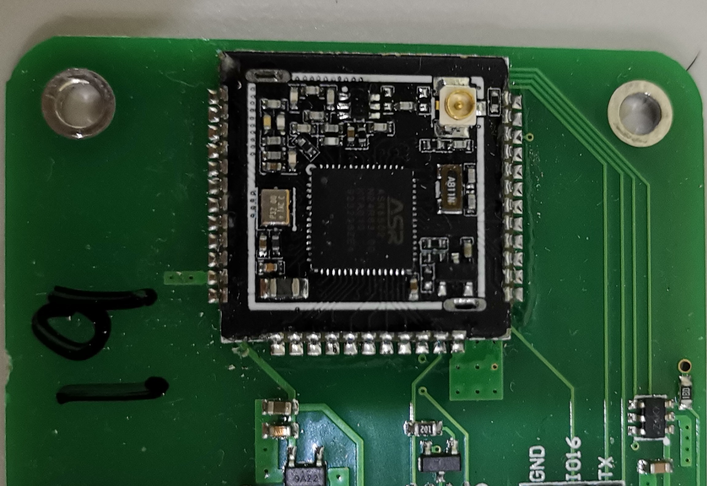
I made this new board. It uses the cubecell module plus.
I’ve found it extremely difficult to reflow properly. Granted I am using KiCAD and thus made my own footprint, but it is a 1 to 1 direct copy from the Altium Footprint supplied by Heltec. The boards looks like this.

I found it extraordinarily difficult to reflow properly. I think this stems from three problems.
- It’s big, you can’t place it precisely with a regular tweezer. You sort of have to do ur best guess, then push the corners till it sorta aligns. Of course, when it’s on the solder paste, it doesn’t really want to move.
- The pads are really close together. I got like 6 or 7 shorts after the reflow process. It may be due to the fact that half of the pads goes underneath the module, and the extra solder paste shorts it.
- It’s heavy. So heavy that it can’t adjust its position during the reflow process like other components do.
Has anyone else met these problems? Any tips? As far as I can tell, this module would cause too many manufacturing issues for production at scales of thousands.