AM02 Module Plus - Custom PCB - Minimal circuit arduino compatible

My implementation is as follows (RST goes to ASR6502 pin #33, PRG to pin #14)
RstPrg

I wanted to keep the programming/reset circuit as simple as possible. In my case programming is normaly done only once while AM02 is used in the end device. Holding both reset and programming buttons down and releseasing reset first, then MCU goes to bootloader and you can upload your binary.

Many adapters have also 3V3 output, in my case I use 3V3 from adapter to power up the device during programming. If you want to make the circuit even more simple, the reset button can be left out. Then just hold down program button and switch power on when you want to enter programming mode.

For program development it is easier just use the Cubecell development board, it has built in USB-interface with automatic reset/programming feature.

I use this kind of CP2102 based USB-TTL serial adapter for programming AM02:
PrgBrd

Hi @arit, thanks for sharing you diagram. I will make my new shematic with your recommandation especially if you confirm to me that only these pins (RX/TX/3.3/GND/RST/PRG) are necessary for flashing. I thank you for sharing to the community your experience.

I order a new CP2102 based USB-TTL serial adapter, I think you propose a good solution for reducing component usage on custom PCB’s.

I also order +5V coils for testing induction charging. I will share my next schematic when orders will be shipped.
Thanks again

Works at least in my case. Here is a photo of the final product PCB:

I use mainly PlatformIO as a development platform but I have tested also that Arduino IDE works with program binary upload. Just bear in mind that you have to activate the bootloader manually holding RST and PRG buttons down, then release first RST then PRG and then start upload.

As I mentioned earlier you can even leave RST button away. Then you have to keep PRG down when device is powered on to enter bootloader mode. In this version of PCB I have also a header pin for reset (RST), it is there just to make it possible to leave reset button away but still make it possible to use hw reset if needed.

3 Likes

Hi @arit, your post inspire me to simplify my next PCB design. I need to flash one time my CubeCell module too, so externalize the flashing circuit and reduce components are good to me.
My project will be placed in a waterproof case and verry probably resin sealed.

As PCB design is not my domain, your picture are quite inspiring on design like ground planes, components position, vias positioning, circuit simplification.
I let you know advancement for my project if it can help community.
So for my next PCB I will use this external USB-TTL serial adapter, I order pogo pins and I will flash on probe points. To substitute the only button (RST) and to keep in mind that my project will be sealed, I order some reed switch normaly opened, wich close with a simple magnet. I have continuity with a small neodym magnet at 2cm.

Someone have an advice for designing an external SMA connector. 50ohms traces, method to inactivate the native µFL module connector ?

I’m also waiting for +5V coils for wireless induction charging.

Thanks!

Hi to all,
a little update for @arit and a question for @jasonXu.

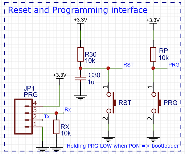
I use the proposed circuit above and all works very well for flashing my custom pcb and adapt for enclosing my device and make it waterproof. So @arit thanks for your advice! This is the choices I made :slight_smile:

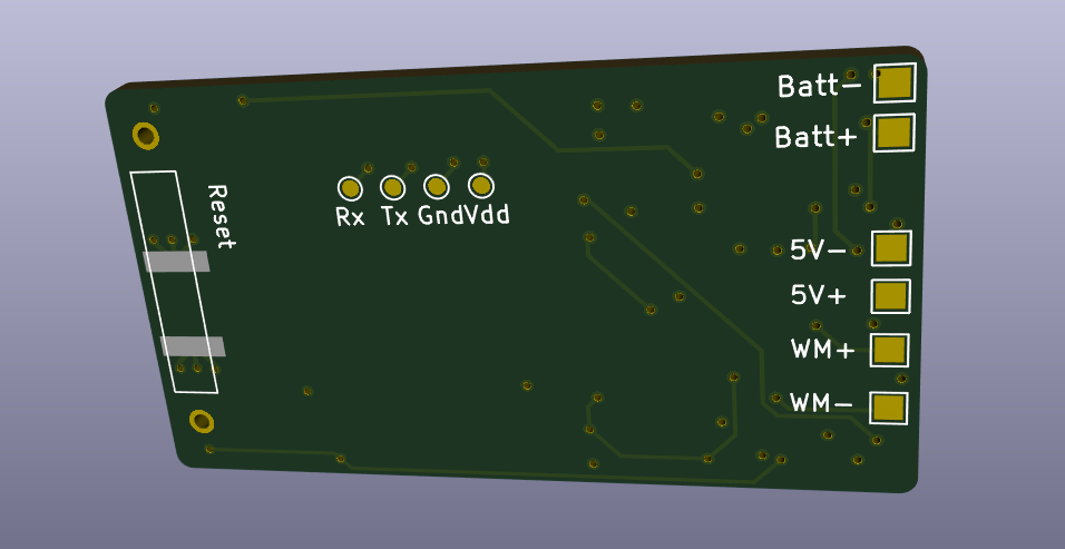
-Instead a button for Reset, I use a reed switch. When I want to reset my PCB without opening the case, I use a magnet.
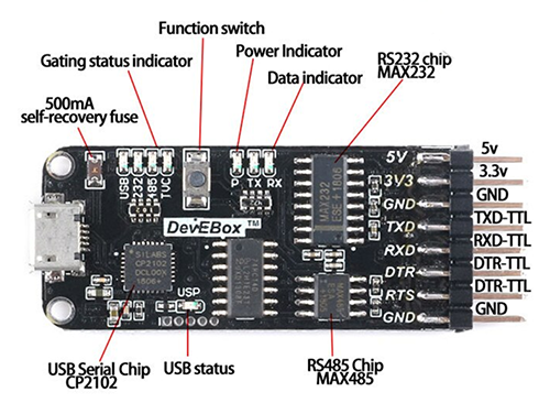
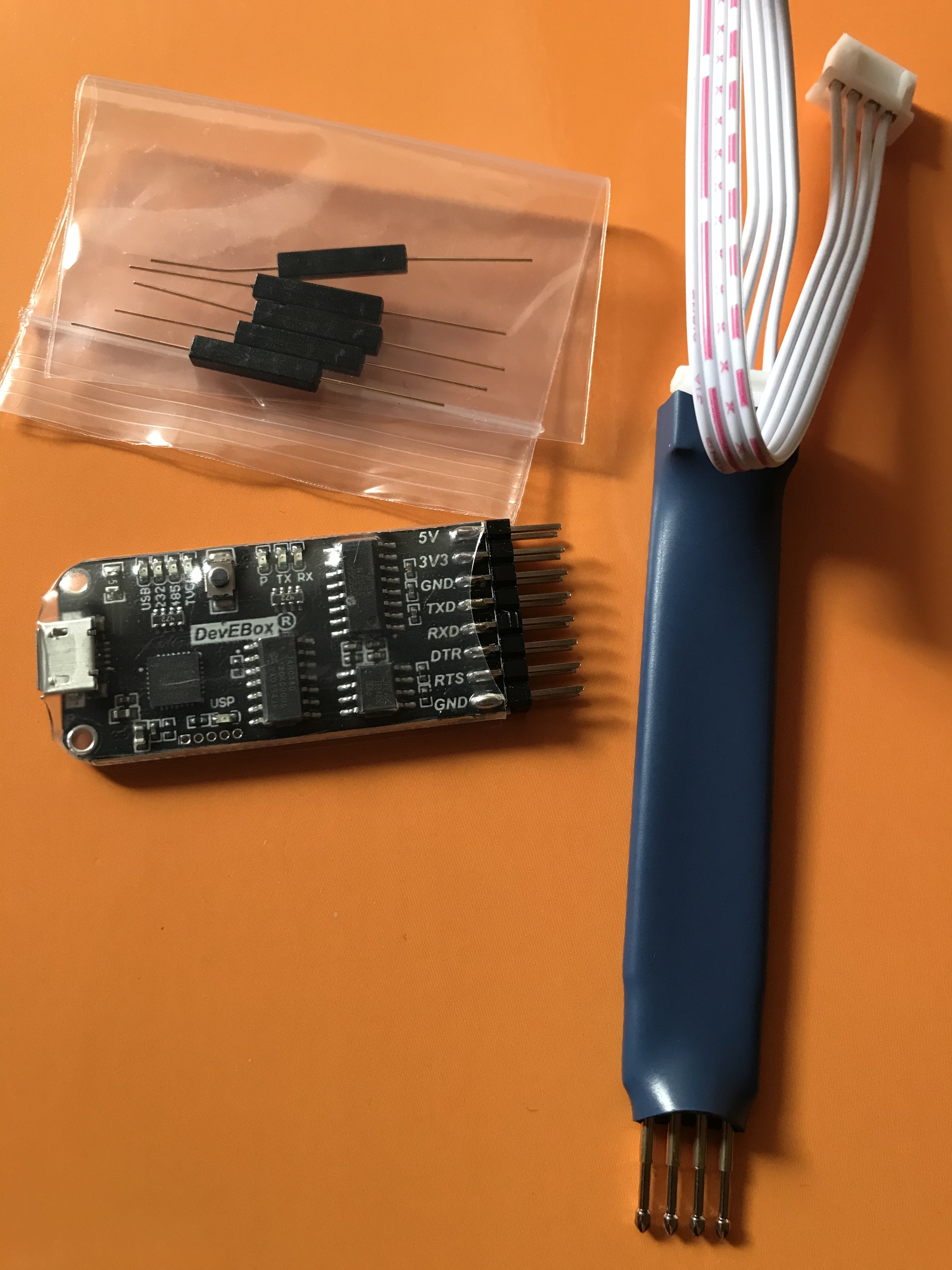
-I design 4 tests points on my PCB and flash it with my 4xPogos pins on my last picture.
One of my mistake was to place a physical button for the PRG pin. On the next prototype I will use a simple jumper (reduce cost and increase ergonomy for flashing)

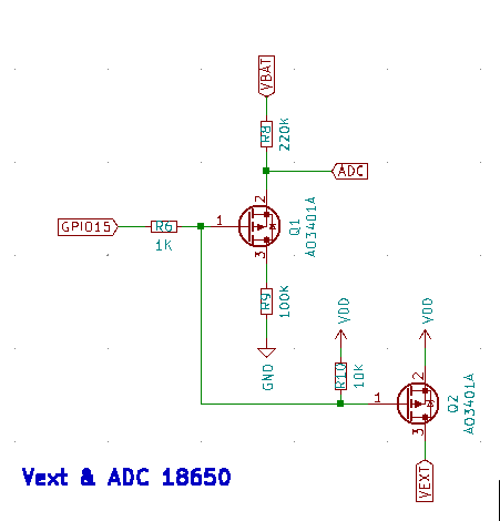
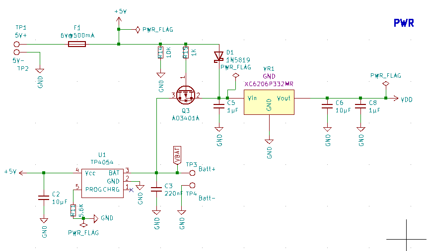
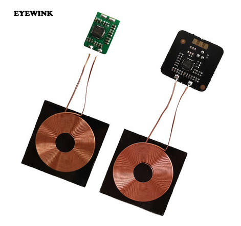
For power management I use the TP4054 for charging a 18650 battery. Instead of using a solar panel, I use a 5V induction charging coil wich permit to charge the device without opening the case.

For the next PCB (and I hope with a new module :slight_smile: from Heltec) I will try to make a good RF section, as I am not a specialist it’s like black magic to make an external SMA antenna connector. I desolder the 0ohm resistor near the µFL connector on the module and I design on Kicad an SMA board edge connector with 50ohm impedance trace. I simply solder a 868MHz helical antenna on the positive side.
I will also take more time to place the tests points for flashing.

For @jasonXu, I want to use another temperature sensor (actually SHT31) wich consume current for readind humidity that I don’t use. @ksckung proposed advice me for powering my sensors on http://community.heltec.cn/t/custom-pcb-htcc-am02-on-kicad/3376/12

What kind of temperature sensor (SMC component) could you propose for the lowest consumption and avalaible libraries (maybe some of Heltec boards have temperature sensor with low power consumption.

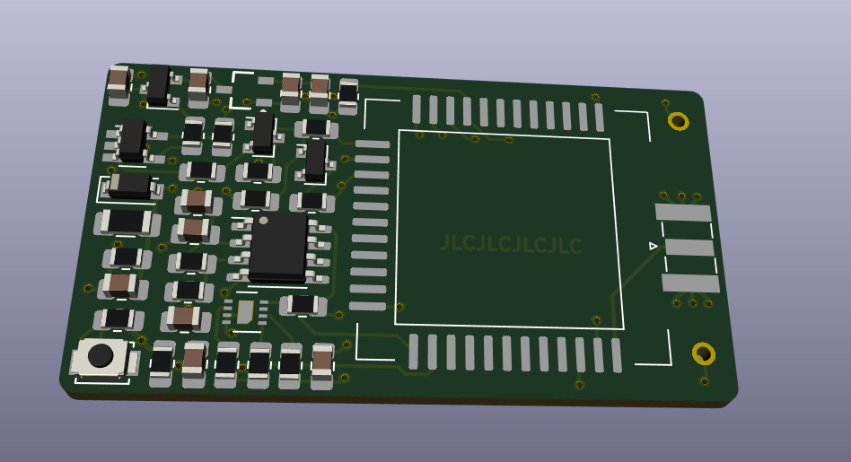
This is some picture of the PCB 4 layers (newbie here, if someone see obvious design mistakes please let me know because there is a lot of stuff to know about pcb design).

Capture%20d%E2%80%99%C3%A9cran%20du%202021-06-01%2022-48-07 Capture%20d%E2%80%99%C3%A9cran%20du%202021-06-01%2022-44-15

I hope it will help someone as you guys helped me for my first newbie PCB design!
Can’t wait to see next modules from Heltec!


HDC2080, Average at 1 measurement/second temperature only, just 0.3uA average current consumption while conversion is in progress.

It is expensive but much faster than HDC1080 and other sensors. That means your device can finish the sampling(conversion time) and back to sleep ASAP.

Configure the HDC2080 to sample temperature only and fewer digits (9-bit accuracy) will also decrease conversion time.

If the sampling period is much longer than 1min. I recommend power the sensor via Vext FET.
Use Wire.end() to terminate the I2C bus and Cutoff the Vext power between wakeup.

Hi @ksckung, I definitvely use this sensor for my new revision of my PCB. Thank you for the advice.

I actually doing test for battery autonomy. It seems that with or without Vext OFF & Wire.end in the code, my battery is drain at the same rate.
Same result when I send data every 15 seconds or every 30 minutes …

I use the AM02 arduino compatible reference design wich include TP4054 with a 18650 battery. I have a 555timer for pulse reading for an irrometer and an SHT31 both on Vext. The sampling time is verry quick, and I send Vbatt, the irrometer value, temperature, humidity on the payload.

I2C is also connected to Vext, I use the pins 24/25 of the module.
I place the sensors reading of the PrepareTx function based on the LoraWan example.
Do my module really enter in deep sleep or do I have a component that drain battery ?
It clearly needs more investigation…

In my case, using CubeCell – Dev-Board and HDC1080.

It is impossible to tell you module really enter in deep sleep or not without measurement.

Use a 1ohm or 0.1 ohm resistor in series with battery and connect it to CRO will help you a lot.
Like this:

First, start from normal LoraWan example with correct deepsleep. You should be able to get 3.5uA or close to 11uA like CubeCell – Dev-Board.

Next, Getbattery example
I may have issue too.


Next, connect the sensor, get the reading than sleep. Check the deepsleep current again. If the current is unexpect, check the current of sensor power, voltage of resistor( check current via that resistor) i.e.: I2C pullup. Vbat voltage divider.

Finally, send the value via Lora, same process.

Hi, I’m going to buy a small oscilloscope to mesure, it will take some days to come.
I only have a simple multimeter for now but maybe I could make some mesurements or changing some parts. (binocular&micropencil solder&hot air).

This is what I was able to make as circuit and handsoldering with the document based on HTCC-AM02_Reference_Design(Arduino).pdf
The circuit Heltec propose is different from the one on dev boards.

Real noob here, I try to understand electronics with this project by making a PCB and obviously some mistakes. Again thanks

2

To get Vbat on ADC, you need to pull low GPIO15 to turn on Q1 PMOS.

When the GPIO15 is low and Q1 turns on, the voltage on ADC will be equal to a voltage divider on a 220K+Ron+100k network.
When the GPIO15 is high and Q1 turns off, the voltage on ADC will be equal to a voltage divider on a 220K+ “ADC pin internal resistance” network.

Toggle GPIO15, measure and study it.
1)
Measure the voltage on the ADC pin by changing GPIO15.
2)
You can cut the ADC trace(copper) and measure the current drawn into the ADC pin.

Question: Is it match what you expect and calculation? Did the voltage within the ADC spec?

Please check the post I posted before and found the solution.

Hi there, I’m starting mesuring my PCB with the LoraWan simple example.
This is the code I put on the PrepareTxFrame function and on the setup.

/* Prepares the payload of the frame */
static void prepareTxFrame( uint8_t port )
{
digitalWrite(GPIO15, LOW);
delay(10000);
digitalWrite(GPIO15, HIGH);
delay(10000);
digitalWrite(GPIO15, LOW);
delay(10000);
digitalWrite(GPIO15, HIGH);
delay(10000);
digitalWrite(GPIO15, LOW);
delay(10000);
digitalWrite(GPIO15, HIGH);
delay(10000);
appDataSize = 4;
appData[0] = 0x00;
appData[1] = 0x01;
appData[2] = 0x02;
appData[3] = 0x03;
}
void setup() {
Serial.begin(115200);
pinMode(GPIO15, OUTPUT);
digitalWrite(GPIO15, HIGH);
#if(AT_SUPPORT)
enableAt();
#endif
deviceState = DEVICE_STATE_INIT;
LoRaWAN.ifskipjoin();
}

Results are for questions in 1 you propose :
GPIO15 HIGH : GPIO15=0V and ADC=3.7V (actually 3.9V at the battery)
GPIO15 LOW : GPIO15=1.6V and ADC=1.2V

For reading Battery I usaually use that I read on this forum.

uint16_t ADCvoltage = analogRead(ADC);
uint16_t BattV =0;
BattV = ADCvoltage*(220000+100000)/100000;

After reading the posts, it seems that resistor values was not adapted for deep sleep and you choose values to reduce consumption. Maybe I choose wrong values for the voltage divider (need to read electronics basics to!)
For the next step I will try to mesure current consumption in deep sleep with battery.
I need to cut the trace connected to ADC and mesure in Amp mode on the section?

Thank you!

Cutting the cooper trace between ADC pin from the module and Q1 and mesuring current indicate 1µA after the PrepareTXFrame (=in deep sleep).

Please make sure which condition is the ADC working by measure the voltage across the resistor(which means current flow through it).
It is no sense that you send digitalWrite(GPIO15, HIGH); but the output pin is 0V, right?

image
Also,Vth of PMOS is -1.3V max,Vbat 3.9V-1.3V=2.6V, GPIO15=1.6V is not high enough to turn off the PMOS, right?

In a normal voltage divider, 220K+100K, if the input voltage(battery voltage) is 3.9V, the output should be 3.9*100k/(220k+100k) =1.21V.
This means when the Q1 PMOS is on, ADC pin should be around 1.21V.

The 3.7V is over the ADC spec. , the current drive into the ADC pin should be much higher than 1uA.
https://heltec-automation-docs.readthedocs.io/en/latest/cubecell/frequently_asked_questions.html
image

Please check what happens when ADC pin following this connection.

For the program, maximum value of uint16_t is 2^16=65536. Did you think (220000+100000)/100000 is ok for this data type?

I retry mesurements and I was mesuring wrong pin ^^

When GPIO15 is low (0V), Fet is off and I have 1.2V on the source and drain pin. Battery reading seems good.
When GPIO15 is high(3.3V), Fet is on and I mesure 3.7V on the source and drain pin. Vext is off.

As you can see real noob here but all your adivces help me a lot.
For the program, maybe using float will be good.

The diagram you propose present ADC connected to D1 but on the one I’m using, ADC is connected to the source.

What’s the difference between both diagrams ?
I’m going to try to mesure total current consumption tonight and redo the code.
Why do I get 3.7V on ADC pin with a recommended design? Can it cause damage to the input Pin ?
Thanks again!

PMOS control logic is inverted.
When GPIO15 is low (0V), Vgs is 0V-Vbat=-3.9V, PMOS is ON
When GPIO15 is high(3.3V), Vgs is 3.3V-Vbat = 3.3-3.9=-0.6V, PMOS is OFF
By measuring the voltage on the 100k resistor to see is there any current flow through PMOS.

What’s the difference between both diagrams ?

The difference is ADC connects to different PMOS pin, S or D.

Why do I get 3.7V on ADC pin

ADC pin has an internal resistor to GND and protection diode to Vcc

with a recommended design? Can it cause damage to the input Pin ?

@jasonXu
As the Frequently Asked Questions said, ADC input voltage can NOT higher than 2.4V. It may cause damage.
I don’t know why they didn’t correct it, but you can see the recommendation on the same page**How to use the ADC pin for AnalogRead (ASR6501) **.

Thank you for your response.
So by design, when GPIO15 is LOW, V(ADC)= with my battery 3.7V to 4.2V. I don’t understand with a circuit is propose knowing that ADC can’t support more than 2.4V. What kind of damages can it cause? Maybe more power consumption?

I really want to be sure for my next PCB design and be sure that any mistake is done with the recommended manufacturer design.
I also need to use one capacitive sensor with GPIO as output and ADC and on the Arduino example the simplest way to wire the sensor is to use GPIO as output and ADC for reading. With the 2.4V limitation, how can I use this one? http://community.heltec.cn/t/cubecell-and-second-serial-port/693/9
Thank you to both of you
@ksckung @jasonXu

What kind of damages can it cause? Maybe more power consumption?

No one knows. In my test, it shows 17uA more(153%) when the battery voltage at 4.2V.
I recommend modify the circuit, measure, and share the result before next PCB design.

The IO voltage of AM02 is 3.3V but Arduino is 5V.
The ADC input voltage is limited to 2.4V with 1.2V reference but Arduino is both 5V.

First, you need to test it work/not under AM02 3.3V GPIO output.
Then check the voltage range of sensor analog output.
If it is out of range, use opamp to buffer and attenuate the signal.

At least, I know how a voltage divider is used! I am disappointed to use the HTCC-AM02 wich is pretty sexy for low power and 3xADC pins.
I’ll try to test my sensor with GPIO as input, maybe it will be a success.


For now, I made a circuit with another circuit with a 555timer. It seems that reading the sensor resistance is more reliable instad the frequency reading and need less conversion to get the value. Too bad … Opamp is also a new domain for me, hard to start from scratch.
I hope that Heltec can improve the ADC input voltage to a more usable one >2.4V (like Arduino’s) on the next modules they produce. Maybe they will tease a date or specifications !
Again @ksckung @jasonXu thank for your help!

@ksckung
I mesure yesterday, it seems that I have 17µA consumption with a 3.8V battery.
Maybe I should try to replace resistors on ADC channels with 10K as you propose here and mesure again.
http://community.heltec.cn/t/power-consumption-in-sleep-mode-vbat-battery-powered/2889/5?u=alexfr

For my sensor, I find a device that I want to design on the PCB. No idead what’s in the black box!
https://www.irrometer.com/pdf/supportmaterial/sensors/voltage-WM-chart.pdf
https://www.irrometer.com/pdf/sensors/405%20Voltage%20Adapter%20&%20Isolator-WEB.pdf
https://www.emesystems.com/smx/documents/SMX_2018.pdf
They said in the doc

ELECTRICAL:3.2 - 30 volt, 1.5 mA input, polarity protected / 0 - 2.8 volt output, linear / 0 - 239 cb (kPa) = 0 to 2.8 volts linear. "

I will post news if my power consumption goes to 17µA to less.
Take care.