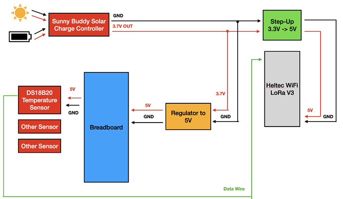
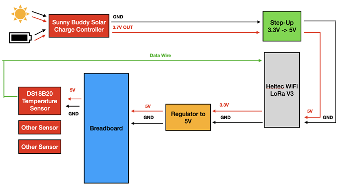
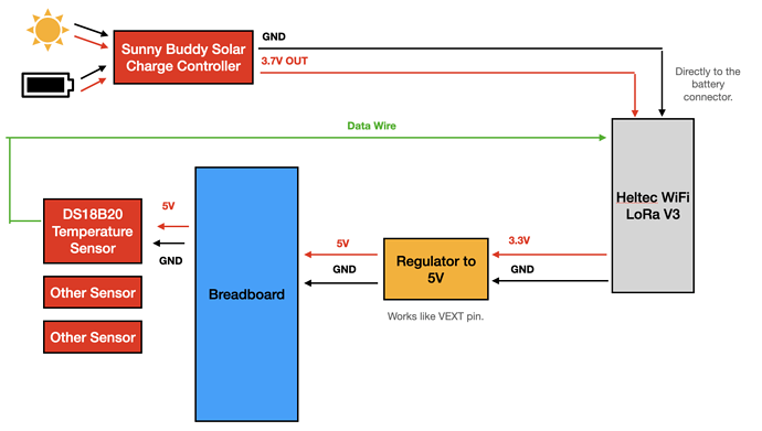
That thing is resetting every 60s like a Swiss watch… 60 seconds delay + 5~6 seconds for joining. Clearly not behaving. Are those screenshots with connections to 5V or Vext?
WiFi LoRa 32 V3: Send sensor data via LoRa, then go back to deep sleep
The connection was with the Vext on the Ve pin (pin 3 on Header J2). If I power via the 5V pin, everything runs smoothly without resets.
Quite sure that powering up the voltage regulator (= enabling Vext) causes a power spike that causes a brownout reset. Do you have capacitors in stock? They may be able to help.
Otherwise you’ll need to get a regulator that takes battery power and uses an Enable pin.
I recently got hold of these. If you’re really under a deadline and can’t wait a week for UK customs, I may be able to ship you one straight away from the Netherlands. They work like a charm for me.
Yes, the Vext goes straight from 0V to 3.3V, and then takes a bit to go back to 0V. I have to ask my Dad tomorrow if he has any capacitors here, then I’ll try that. Luckily my deadline is not that tight but thank you nonetheless for the offer. 
The problem is that enabling Vext allows instant flow to the voltage regulator, which causes a power spike, and happily consumes all the power it can get, as it can’t sense the load for the first few milli(micro?)seconds. And as the power flows through the board itself, there is not enough power left for the MCU. Causing the full reset.
So you can only use Vext for 3V3 sensors, not for a regulator. Batteries are usually more capable of handling these spikes, and the power for the MCU is delivered parallel to the regulator load. So there’s no brownout reset.
Okay, thanks for the explanation! That’s kind of a pain though, my plan was to use the Vext pin so that the sensors would also be off during deep sleep to reduce the power consumption (why does everything these days have a bright blue LED?!  ). But that’s where the capacitor would come in helpful, if I understood you correctly, right?
A capacitor may be able to dampen the power spike. Enough examples on Google on values and connections.
But the regulator I listed has an “Enable” pin, which works exactly like the Vext_Ctrl pin. When not enabled, the complete load of regulator + sensors on my multimeter shows 0.0 uA, it’s not even able to measure it (at least lower than 1 uA). And it outputs 5V up to 200mA as well, with input taken from battery.
Quick note that with a decent bit of care and small screwdriver, you can decapitate LEDs as well. But at your own risk of course.
Thank you for the explanation. If we have a capacitor at home, I’ll try that and report back whether there are any improvements.
So I could connect the regulator to the 3.3V pin of the board, and then from there connect the sensors, right? That seems good. When I’m back at the university on Monday I could ask if we have something similar there.
The new PCB that was designed for another project but also with my sensor suite in mind will arrive somewhere near the end of February I think… looking at the schematic, there are enable pins, which is good… also everything including the controller is on the same PCB, so the power supply for sensors should be turned off when in deep sleep.
But with a capacitor or a regulator I could test the code first, which is important.
This depends on your regulator. Ideally, you want to be able to ignore the board completely and power the regulator straight from the battery. That thing is designed for certain spikes (some do 2A, others 4A, …), your board is generally designed for 500mA. The 3V3 pin may be able to handle a spike better than the Vext pin, but bypassing it completely is the better choice.
That would however require your regulator to be able to take the complete voltage range of a battery (2.7 - 4.2V generally). You would have to check if your regulator is 3V3 only or supports the whole range.
Okay, thank you for the explanation!
I guess my connections would then have to look more like so:
By-passing the pins on the board entirely:
Using the 3.3V external sensor supply pin on the board:
(again, sorry for the not very electrical engineering standards like drawing)
No no no… there’s a battery header on the back of the board - that thing actually has a charging IC included and takes 2.7-4.2V. You don’t need that 3V3-5V booster towards your board’s 5V, hook ip to the battery port instead.
Heck, with a decent 6V solar panel you should even be able to skip the Sunny Bro and hook that panel up to 5V, which the device will use to charge the battery!
But either way, skip that regulator to the board!
I see the battery header, but the standard connector of my rechargeable battery does not fit with that at all. My solar panel has a peak power of 18.3V and 1.64A, so I definitely need the Sunny Buddy there. I have also measured and estimated that the MPPT point is at 3.7V, so that’s also the max output I get from that controller. I don’t think I can skip the regulator to the board, unless the board can also be powered with one of the 3.3V pins. This document by the manufacturer says that pin 2+3 on header J3 are 3.3V power supply pins, but to be sure I will test if I can actually power the board via these pins.
I’ll get back to you with more info and results tomorrow; I’m heading to bed to recharge myself now. 
Your board should’ve come with an appropriate JST cable. You can cut the connector from your battery and solder the JST connector on there, and plug it in. Really, whatever step you can throw out of the equation is 100% worth it in the long run, especially on battery power. Although that is a quite massive solar panel… but if part of the project is low power, then that booster is going to raise a lot of eyebrows.
I took a look at the schematics of the Sunny Buddy and the WiFi LoRa V3. The load connector of the charge controller is connected in parallel to the battery. If the solar panel provides such a high voltage, I see no chance to avoid the controller. The WiFi LoRa board feeds the nominally 5V from USB (VBUS) to a TP4054 (max. 9 V input allowed) for charging the LiPo and to a CE6260B33M (abs. max. 8 V input allowed).
But I see no problems with connecting the load output of the Sunny Buddy to the JST connector as the only power supply of the WiFi LoRa. Both the CE6260B33M and the AO7801 MOSFET for VEXT on the WiFi LoRa should be able to supply around 500 mA in total. This includes the power consumption of the WiFi LoRa itself. I think it is not a good idea to power a boost converter directly from VEXT (inrush current problem).
I would rather use some GPIO pin and connect it to the gate of a P channel MOSFET (e.g., AO3401) to switch another connection from the positive pin of the load terminal from the Sunny Buddy on or off. I would pull the gate of the MOSFET high with a high value resistor (e.g., 100k-10M). When invoking sleep, you could set the pin mode of the control GPIO pin to high impedence (HiZ) or INPUT, but this not needed for most GPIO pins, as they will normally be HiZ in deep sleep anyway. A HIGH, or better yet, HiZ on the control GPIO pin disables the external power supply, a LOW enables it. Then, you are free to do whatever you want with the switched power supply, you could use an LDO for providing 3.3 V to the sensors and breadboard, or you could use a boost converter for supplying 5V. And the sleep current should be extremely low.
Thank you for your reply! I think I will add the MOSFET to the VEXT, that was my original plan, I just had gotten the wrong one as the Heltec board is using plus rather than mass, which is what I had expected since it’s the standard. I will order these MOSFET then and test them.
Edit: They are not available in single quantities at any seller here…
Yes, a MOSFET is a good idea. But there are N channel and P channel MOSFETs. If you use an N channel MOSFET, it is used as a low-side switch, so it switches GND (negative) on and off. In this case, you need to make sure that there is not other GND connection between your sensors/breadboard and the WiFi LoRa (e.g, through data lines), otherwise the external components might not switch off correctly. To switch such a N channel MOSFET on, you would pull the gate to the HIGH state, e.g., by connecting it to VEXT.
Due to the problems with other negative connections, I suggested using a P channel MOSET. This can be used to switch the positive rail (high-side switch). I think this would be safer in this case, since I have no idea what is happening on the other connections (data) between the sensors/breadboard and the WiFi LoRa. But you cannot connect an P channel MOSFET to VEXT. To switch the P channel MOSFET (like the AO3401) on, you need to pull the gate to GND (negative), i.e., set a connected GPIO pin to LOW. So, you need to use another GPIO for the gate, not VEXT. The source pin of the P channel MOSFET needs to be connected to the positive battery terminal (or the positive load terminal on the Solar Buddy), the drain pin of the MOSFET needs to be connected to the positive (Vcc) input pin of your voltage regulator or boost converter. The drain pin acts like a switched positive battery terminal now.
Thank you for the explanation.
Could you perhaps, if it is not too much work, add a connection diagram (can be a rough sketch like what I attached previously in this thread) and some code? I’m having a hard time understanding how I should connect all of this.
From the pin map, I see that on the board, GPIO 45, 46, 48, and 47 only have the GPIO function, so they seem safest to use for this purpose. Should the GND go to a GND pin on the board or on the Sunny Buddy? The P channel goes directly to the Sunny Buddy. Other than that, I am confused.
Thank you already in advance!
If I may ask, how would you connect this one? I assume that I need a GND and power supply, either from the Heltec board or directly from the charge controller. And then I could connect my sensor suite to the regulator, right?
So one possible scenario would be getting the supply for the regulator from the board, right?
And the other would be getting it straight from the battery, right?
Thank you already in advance for taking your time to explain!
Yup, either is a valid schematic, but the latter is, as mentioned before, preferred if there are no other factors at play. Anything you can wire up in parallel means less chance of failure down the road.
Of course you’d also need to add the Enable wire.
Thank you! Where would I connect the enable wire? That one has to go to the board, right? Is there a specific pin I should/could use?


