Power supply pin on HTCC-AB02

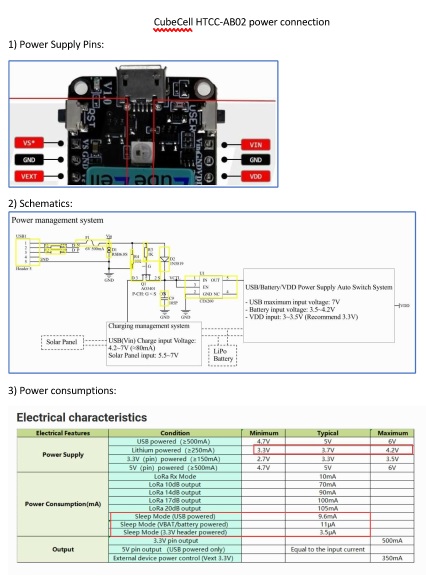
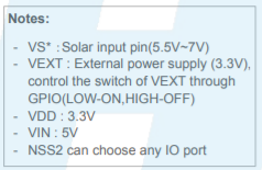
I have questions about the power supply pins of HTCC-AB02 board: Based on Heltec web site, I found the schematics, pin out and power consumption of AB02 board (attached). My question:

  1. Is there a description for each of the 4 power pins: Vs, Vext, Vin and Vdd?
  2. The schematic does not show the details of the two power management blocks. Is there a detailed schematics for the two blocks on the schematics?
  3. On the electrical characteristics chart, what is pin of the “3V header powered” (with 3.5 uA) in sleep mode?
  1. Just on the left side of pdf
    Vin is connect to USB 5V
    Vdd is connect to LDO 3.3V output and power the whole system
    Vext is connect to LDO 3.3V via a PMOS controlled by GPIO.
    image
  2. It is a TP4054(or equal) charging circuit where TP4054’s Vcc connect to
  • Vs
  • USB 5V through a diode
  1. Vdd 3.3V which is the System power. It also means that bypass the LDO and ignore LDO’s quiescent current.

Thanks. This is very helpful.

One question: is the LiPo battery plus terminal connected to the input of the LDO (U1 CE6260) via Q1 (AO3401)?

It is a hidden block and I do not have AB02.

On my AB01, It is the same as you stated.
More information, the Q1 Gate connects to USB 5V via 1k resistor to switch off Q1 when USB powered and Vbat charging via TP4054.

You can found some hint in other heltec product’s schematic.