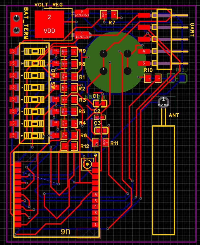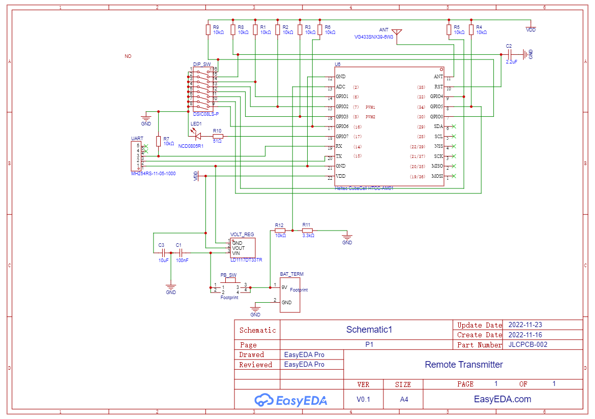
I am almost at the stage of getting a PCB made for the cubecell.
This is my first time designing a pcb, so I am not sure if I have done everything correctly or not.
A couple of questions:
-
Is it okay to run traces underneath the CubeCell module, or do I need to keep that area clear on the top? I have kept it clear where the solder is from the shield.
-
should I be modifying the trace width from standard for the antenna trace? does this need to be kept to 50 ohms? If so, is there an easy way to calculate the impedance at 433MHz, based on trace thickness and length?
-
I intend to program with Arduino IDE. Am I correct in assuming that all I need are the RX, TX and GND connected to a UART to USB converter cable?
Sorry about all the newbie questions, but this is a steep learning curve for me.
Thanks