Heltec wireless tracker: 5V part at the PCB defect

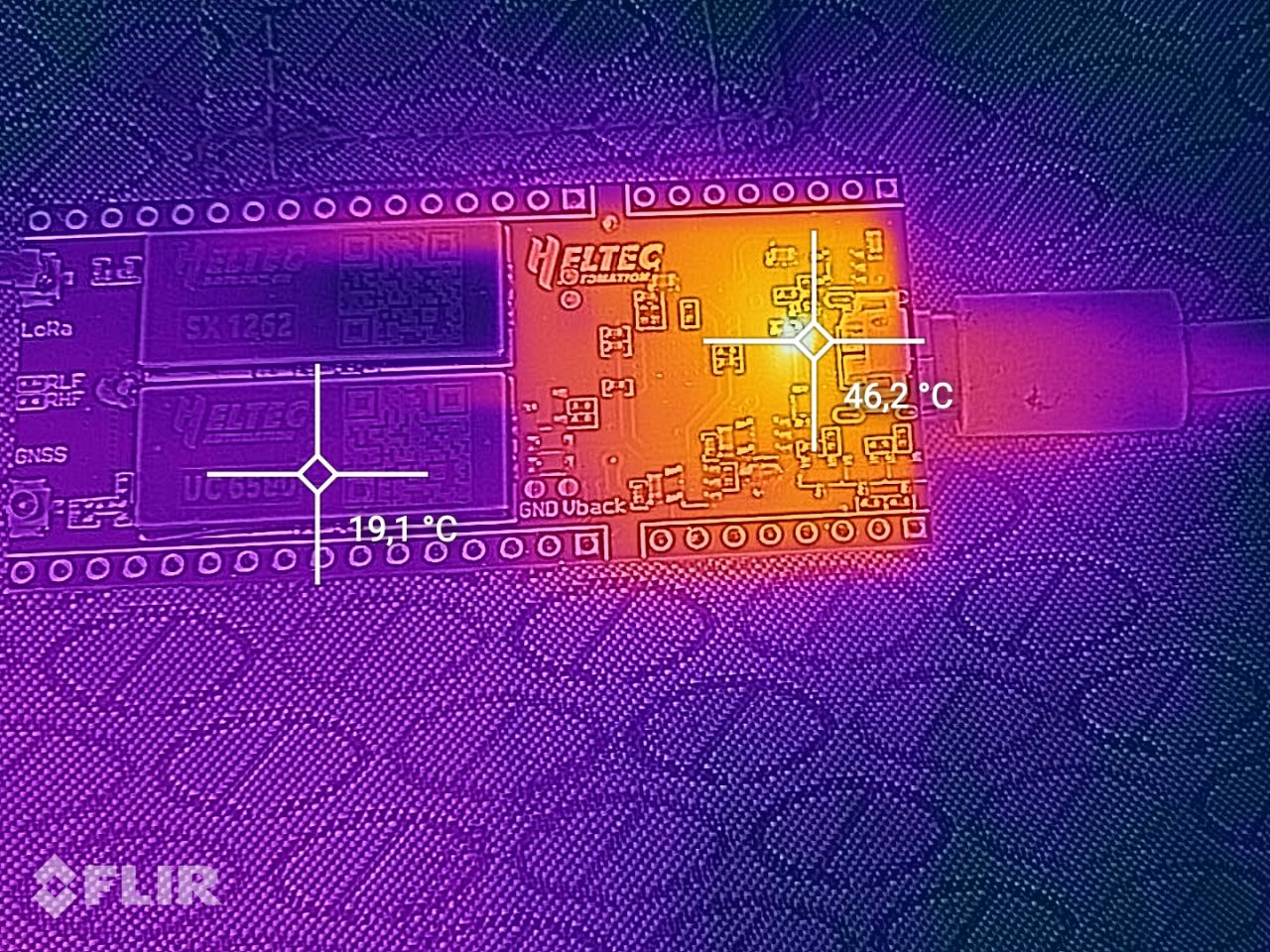
My heltec wireless tracker suddenly does not boot anymore when powered via USB-C connector or 5 V VDD pin.
I tried to power it with 3.7V via battery connector. -> Success, device boots.

Perhaps, an over-voltage of the powerbank or static electricity charge caused an electronic part to fail.

Now I’m searching for the problem in the 5V part of the PCB.
I looked at the schematic.
Possible causes (imho), because they are connected at the 5V line: defect of
a) TP4054 chip
b) D1
c) R1
d) C1

Fail of Fuse F1 is unlikely to have failed, because I tried to power with 5V via pin 1 of header 8.
R2 is irrelevant because it controls the transistor which switches off the line back to the battery from voltage coming via D2 (usb or 5V); battery charging is controlled by TP4054.

My problem:
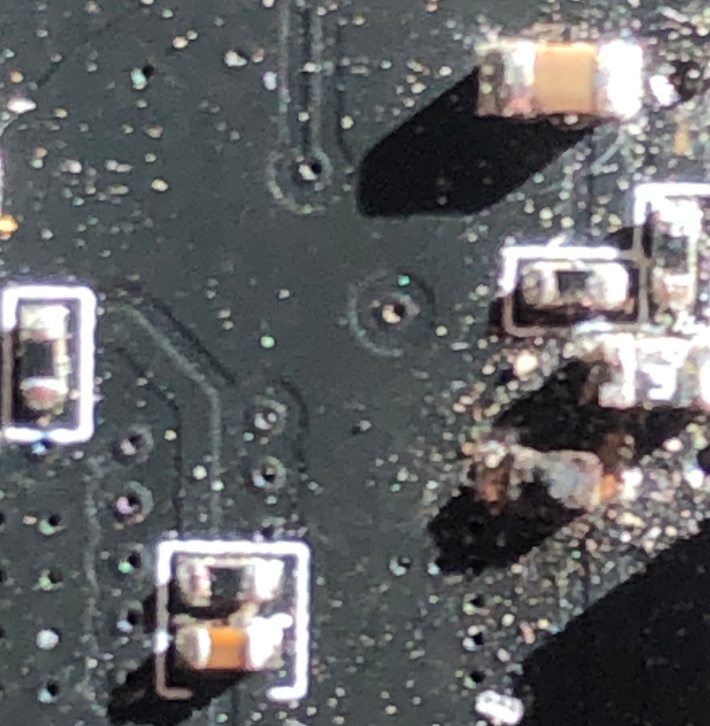
While the schematic diagram is good and the concept is understandable, I did not found a description of where to find the parts on the PCB.

-> I need to know: where on the PCB can I find D1, R1 and C1.

Position of F1, R2, D2 and Q1 would be also of interest.
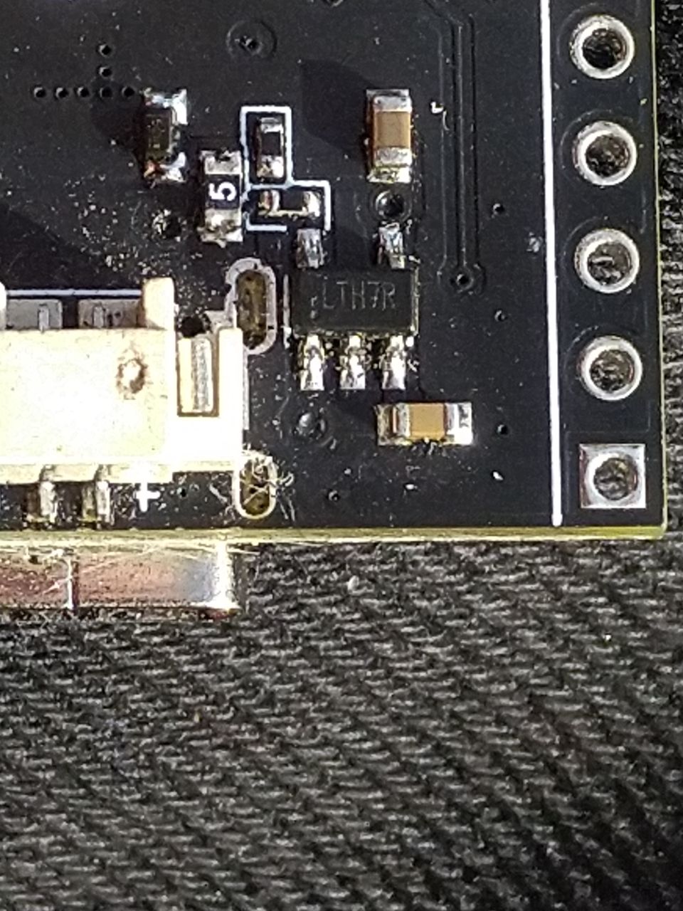
TP4054 was easily to locate (stamped with synonym LTH7R).

  • Thomas

The use of a multimeter will quickly resolve which component has failed by plugging in the USB and checking for voltages around the connector.

The TP4054 has no impact on providing power - it’s only for battery charging - unless it’s shorting.

C1 &/or R1 would need to go short circuit to affect the power input which is unlikely as you generally have to try very hard to do that to those types of components.

However D1 is a transient suppression diode of a design that does short if triggered. So it would be useful to monitor current when powering from USB or the 5V pin.

U4, the 3.3V reg, if it’s been compromised, would be a likely culprit and easy to check for voltage in and voltage out with a multimeter - and relatively easy to spot on the board as it has 5 pins.

Perhaps you could take a high-res picture to help with component identification.

Thank you for your response, Nick.

The TP4054 has no impact on providing power - it’s only for battery charging - unless it’s shorting.

Yes. I assumed it may have failed and had an internal shortage.

With my flir cam I saw the heat here:


The thermal image is not so well adjusted and its resolution is not very sharp

Current was abt 350 mA.

In the mean time, it became worse:
Between 5V and GND I measure 10 Ohm.
Now, if I connect 5V power via pin1 (header 8), or via USB (-> F1 is still alive), the defect part heats much more up, lights (!) and smokes. I immediately removed the power source for not damaging anything, so I had too less time to see exactly which part heats up: it was (again) that one of the both of the thermal image.

Operating via 3.7V header, everything is still fine (device boots up, lora rx/tx and gps work), with low current as usual. -> U4 and U6 operate as expected. D2 still does its job and blocks from that internel <5V line back to the outer 5V power-source-area.

This is the foto with the part labled with “5” and, left of it, the other part; I think the latter one is the smoker. But they are so close to each other…

So remove it and see what occurs.

At worst you buy another charger chip or don’t use a LiPo on it.

Short story:
I was successfull. Device now boots up again when external power connected via 5V pin or via USB-C.
Measured power consumption via USB-C: 94 mA during boot. 148 mA when my firmare runs, and 175 mA when LoRa starts TX. These are the usual values I know from measurements months ago.
And: My usb-serial is still working.

Long story:
From my last picture, it was the part left of that one labled with “5”.
You said “remove it and see what occurs” - well, yes. It was also my initial thought - but I prefered to get a second opinion (yours - thank you!), before doing something really wrong.
I was unsure, because there was one uncertainty: if it would have been “fuse F1” warming up, I would have needed to search the error somewhere else; removal of fuse F1 would have cut power from USB-connector.

In the meantime (test after your answer) the defect part became obviously “ugly”, so it was clear that I’ll remove that one, and not the part with the “5” nearby.

I really would have felt better if there would be a picture of the PCB by heltec available, which describes the parts according ther type/number of the schematic, instead of poking around in the dark.

Thank you gain!

I close with a picture of the obviously defective part (south of part “5”):

1 Like

Good you’ve got it sorted - I’d guess at it being the RSB6.8S transient suppressor which may have been zapped but looking at your first photo where it looks somewhat misplaced on the pads, may have given up early.

I’d not bother replacing it unless you are prone to zapping things with static electricity, wear a lot of polyester or rub balloons in your hair a lot. When I was a lad I spent a lot of time with a lead on my wrist plugged in to a mains socket because you could zap a chip by just looking at it. Nowadays it’s far less of a problem.