A- When GPIO 21 is set to ‘1’: adc2:4 (gpio 13) will read full vbat value (probaly something greater than 3.3V).
B-When GPIO is set to ‘0’: adc2:4 (gpio 13) will read vbat in voltage divider (certainly lower than 3.3V).
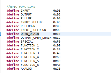
For “A” case, GPIO 13 must be configured as input? Is it tolerant to 4.7V working as input?
Hi! I have been uing this method of battery measurement over the last year (since V2 has been out). The results were never quite reliable, and I assume, that teh voltage divider circuit was not very precise. But is was sort of good enough for my application.
Now I got a new batch of modules, and there were some apparent changes to the circuit (unfortunately not documented anywhere, it seems). The bad news: the method of voltage measurement that was in the example files does not work anymore… Is there an improved way of measuring battery voltage? Can I get hold of any documentation what the circuit actually looks like right now? ARe there new example files available?
Thsi is rather crucial for me - I am shipping out about a 100 kits every month, and as long as this has not been resolved, I am actually stopped in my tracks, as the software I am using will be broken…
Any help is appreciated!
Hi:
I’m sorry we didn’t explain the new changes, which caused you trouble.
As you expected, this PCB change is to change the battery detection pin from 13 (ADC2) to 37 (ADC1). This is to avoid the limitation in the ESP32 chip: When WIFI is enabled, ADC2 is occupied by WIFI can not work.
If you need to continue to use the battery test, just change the 13 in the original routine to 37.
Sorry for the trouble, and I apologize again.
Thanks, Saber, this was helpful. BUT: In my application pin 37 is used as GPIO with external pull-up… this means the value read is meaningless. Further consequences: I have to re-design the schematics and PCB and throw away 700 PCBs I had already manufactured. Further problem: I have to maintain two sets of software releases, one for the >1500 items that are already out in the field, and another one for the new version. VERY disappointing.
To come up with a new release that changes pin assignments without notice in advance, and with the same version number, is very unprofessional, to say the least. Not to mention that there still is no up-to-date documentation (schematics) available.
Honestly, I do not know how to proceed from here. Creating a new version with your un-announced changes incorporated seems to be very risky - how long until you change the specs again? I need a supplier I can rely upon.
We are very sorry for your problem. Because of the power management bug of ESP32 chip, ADC2 and WiFi cannot work at the same time. So we moved the ADC pins from the original GPIO 13 to GPI 37.
This is a terrible upgrade and we did not update the documentation in a timely manner. Such problems will never happen again in the future.
I think, you can continue to keep pin 37 as a GPIO function by turning off the MOS-FET. Is this okay?
I can use GPIO on Pin37, that’s not the problem - but I cannot at the same time measure the battery voltage, because I have an external pull-up resistor on Pin37, so the voltage is always close to 3.3V (and not around 1.3 through the voltage divider); but I also need the battery measurement in my application.
My question is: can I source around 700 of the older modules from Heltec? I still have 700 PCBs that I do not want to throw into the trash (they were expensive!). The WiFi problem with Pin13 does not disturb me - I only use WiFi for OTA and uploading files, and restart the module, before I measure battery voltage again.
Definitely yes, an agent has feedback your question to my colleague this afternoon.
How long is your time requirement? Production takes about two weeks, but January 20 to February 2 is the Chinese New Year holiday. This is a national holiday, and almost all suppliers and factories will stop working.
Hi guys,
I tried to find some sample sketch for reading the battery-level, but the only one i found quite helpful is this:
But looking though it, it neither contains “pinMode(13, OPEN_DRAIN);” nor something about GPI 37.
When i uploaded it to my Lora (V2) the battery voltage seems to slowly drop to zero, and the percentage goes to -45% … I guess it tries to read it from A4, so i changed it to analogPin = 37. But then the display stopped working so i changed it back to A4. Now the display works again but the reading doesnt make sense.
Could you please just tell me the few really essential lines i need?
@Saber I have more than 150 wireless stick lite here with me and I order more 150 to my supplier. I would like to now if the power detection pin is still at PIN 13. How can I check this?
Which is the best method to read the battery before the regulator, and after the regulator ?
With reference to the posts by oe1wkl above about the change from GPIO13 to GPIO37 for battery voltage-divider reads:
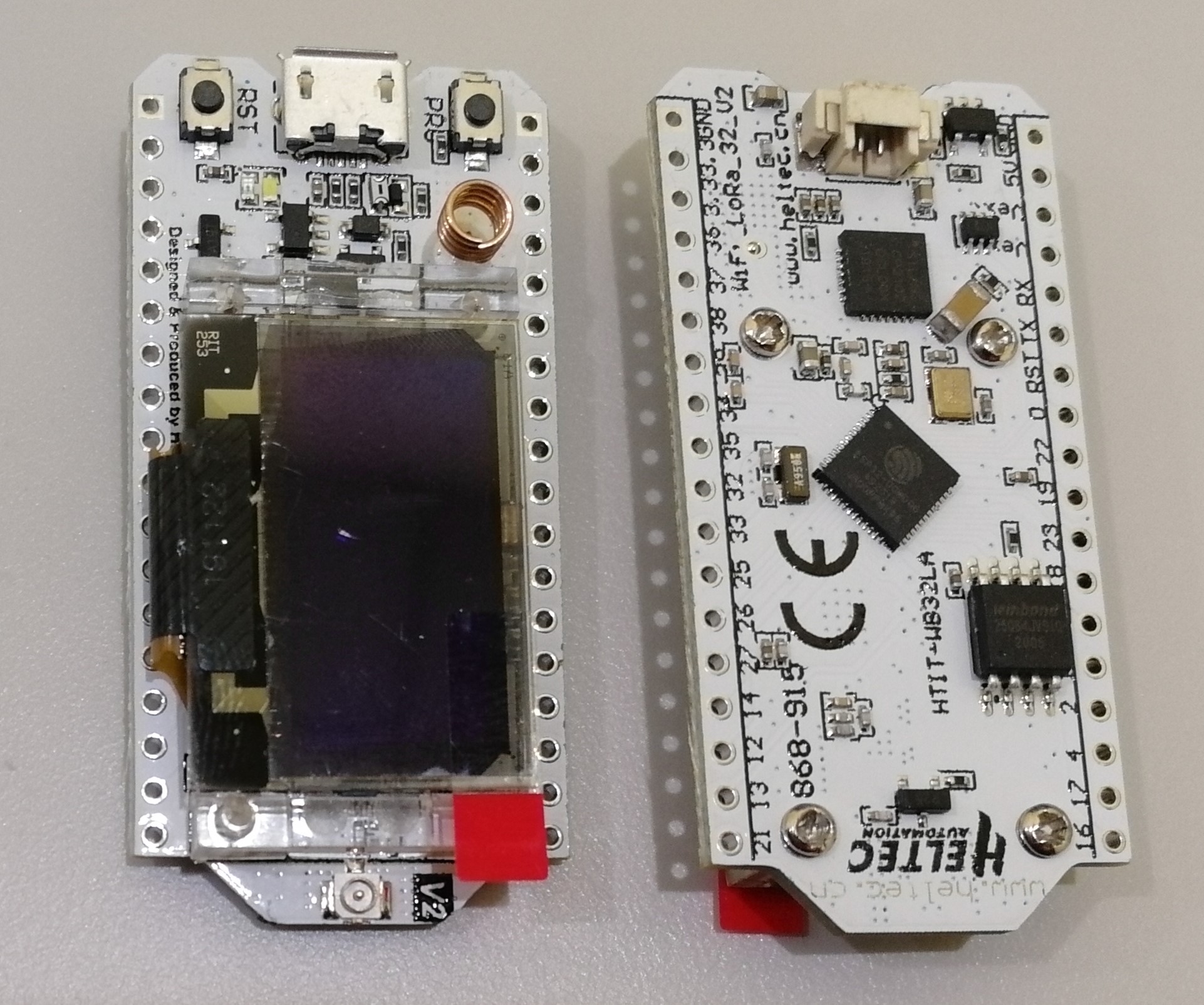
Q. How do we tell what variant of V2 board we have? (i.e. how can I tell which GPIO pin Vbat is connected to)
Given the importance of holding GPIO21 high (to pull the voltage divider to GND and avoid Vbat voltage hitting the ADC ‘undivided’), I want to make sure I know which variant of V2 board I have before I start testing.
I think I just answered this with some DMM (Fluke 289) measurements on my board; for these measurements, I had USB connected together with LiPo (charging), where my Vbat was 4.15V.
When GPIO21 was HIGH 3.3V, GPIO13 was 0V, GPIO37 was 3.58V, Vext was 2.92V.
When GPIO21 was LOW 0V, GPIO13 was 0V, GPIO37 was 1.28V, Vext was 3.3V.
Ignoring the negligible Rds of the AO3401, with the 320K/100K voltage divider, for case (2) I expected approximately 3.2*1.28=4.096V, which was pretty close to my Vbat of 4.15V.
Also, G6EJD has shared a simple ESP32 voltage reading function on github which applies a polynomial correction to the ADC read. Here’s some example output from my test sketch (when my DMM was measuring Vbat of 4.16V:
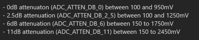
I’ve been developing sketches for my Heltec Lora V2 and working to try to read the battery voltage. I’ve read a lot here that indicates that the internal divider provided (activated by GPIO21 = LOW) tied to originally GPIO13/ADC2_4 and has moved to GPIO37/ADC1_1. I don’t seem to be getting any good values out of mine over about 1.2v (before x3.2 divider). That is on a 6dB gain. I think that means I need to move to a higher gain, even with the divider, but the range for 6dB atten setting says that should go from 150mV-1750mV… I really think I need to know how to determine WHICH version of V2 I have (old GPIO13 vs. new 37)? GPIO13 seems to be at or near 100mV for both states of GPIO21. But I really am struggling with why I can’t get readings that never seem to differ from 1.21v (even with a very low lipo around 3.2v or up to 4.2v).
Somehow, I seem to have things working with the 6dB atten now and I’m using the EFuse compensated internal calibration readings as well for ADC1. I am not certain what was being done incorrectly before (possibly something I had in the ADC setup was setting me at 0dB atten through the various sketches I was trying to copy ADC readings from). I’ll try to clean up what I have working to just demo what I’ve got working and upload sketch.
Also, the V2.1 pinout document is wrong:
It shows labeled 3v3 and GND in upper left (3rd/4th pin from top left), where those are BOTH actually clearly labeled Vext on the board silkscreen on back and I’ve confirmed are = 3.3v when GPIO21 low (see the image below for the silkscreen label that shows it also Vext and Vext):