Hello
I bought several Wireless Shell (V3) modules and made printed circuit boards for them.
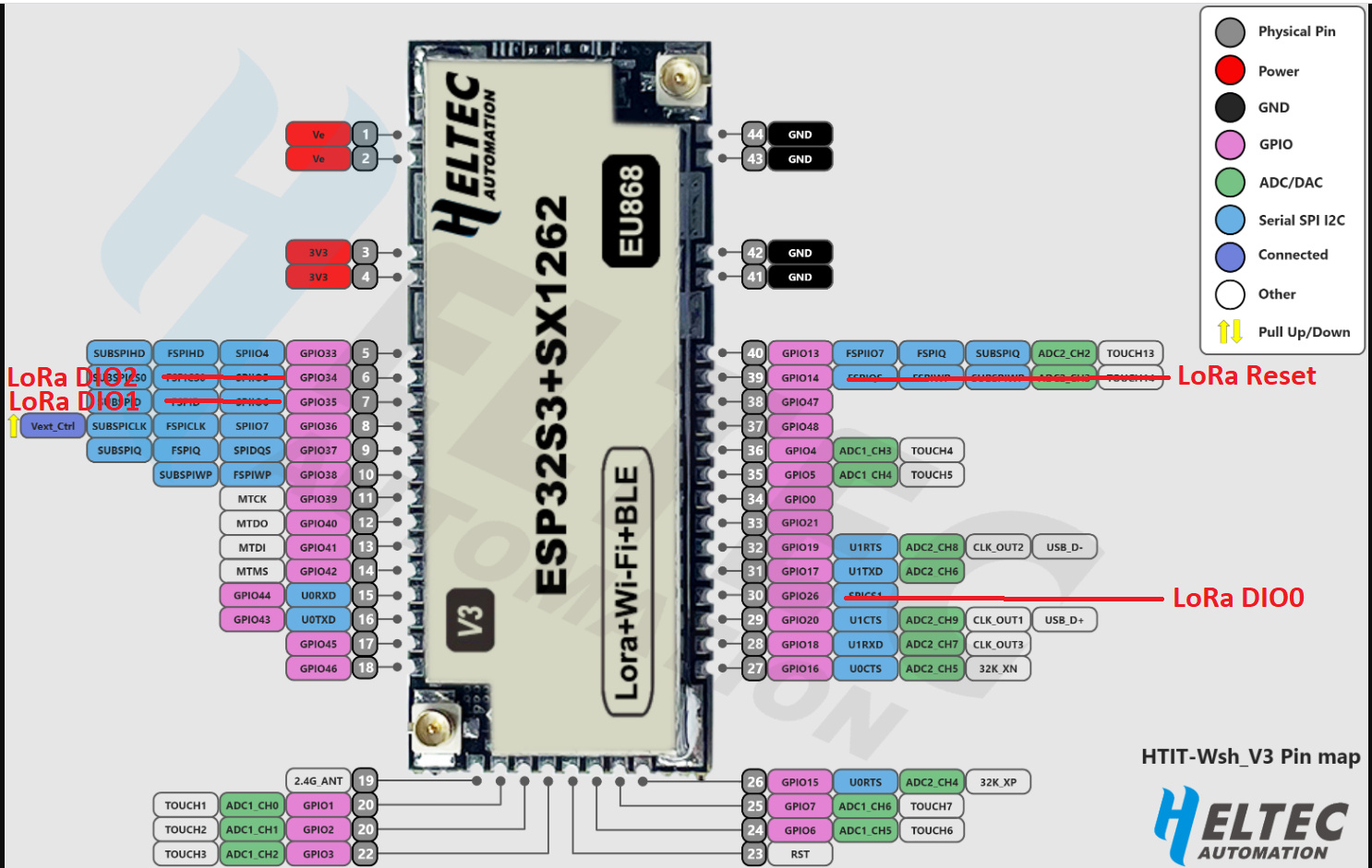
Unfortunately, the pinout diagram from the site is not complete and my boards do not work.
For example, in the pinout diagram, pin14 is free, and judging by the variant.h, LoRa Reset is connected to it
Could you give me the internal diagram of the Wireless Shell (V3) module so that I can do board development
Or give the complete pinout diagram of the Wireless Shell (V3)